The Light Speed Pivot: Why Silicon Photonics is the Future of AI Data Centers
The Light Speed Pivot: Why Silicon Photonics is the Future of AI Data Centers
AI & Semiconductor Industry Analyst | 8+ Years Covering Emerging Tech
The Interconnect Wall: Why Electrons are Slowing Down AI
As the industry moves from training Large Language Models (LLMs) with billions of parameters to those with trillions, the primary bottleneck is no longer just the raw compute power of individual GPUs. Instead, the industry has hit what architects call the 'Interconnect Wall.' Traditional data centers rely on copper wiring and electrical signals to move data between chips. However, as data rates climb toward 224 Gbps per lane and beyond, copper encounters physical limitations: signal degradation, heat generation, and high power consumption.
This physical ceiling has necessitated a shift in hardware architecture. It is a central component in The Evolution of AI-Optimized Semiconductor Architecture. To maintain the scaling laws of AI, the industry is transitioning from moving electrons over copper to moving photons over fiber-optic lines directly at the chip level. This is the application of silicon photonics.
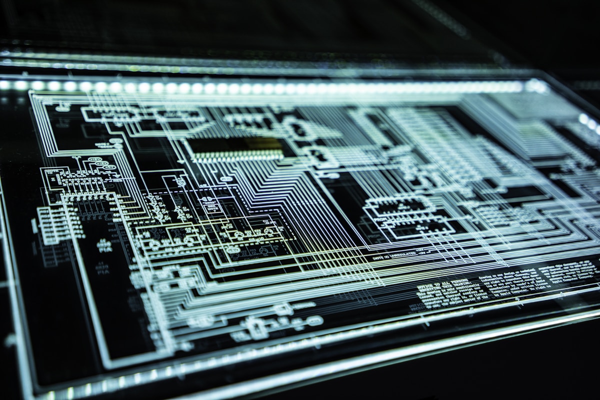
Defining Silicon Photonics in the AI Context
Silicon photonics (SiPh) is a technology that integrates laser-based optical communication onto a silicon substrate. By using the same CMOS manufacturing processes used to make traditional processors, manufacturers can create 'photonic integrated circuits' (PICs). These circuits use light (photons) instead of electricity (electrons) to transmit data. In an AI data center, this allows massive clusters of GPUs to communicate with significantly lower latency than traditional electrical paths.
Unlike traditional pluggable optics, which sit at the edge of the server rack, modern silicon photonics aims to bring the optical engine closer to the processor. This proximity reduces the energy required to drive the signal, addressing the power-to-performance ratio in AI infrastructure.
Addressing the Power Challenge
Power consumption is a significant hurdle for modern AI data centers. A substantial portion of energy in traditional setups is lost to heat generated by electrical resistance in copper cables. Silicon photonics offers a path toward low-loss transmission over longer distances.
Industry developments reflect this shift. For instance, Broadcom and Intel have demonstrated Co-Packaged Optics (CPO) solutions. In a CPO configuration, the optical engine is integrated within the same package as the Ethernet switch or the GPU. This reduces the need for power-intensive retimers required to boost electrical signals over copper, with industry data suggesting potential interconnect power savings of 30% to 50%.
Bandwidth Density and the Scale-Out Challenge
AI workloads require intensive 'all-to-all' communication. During the backpropagation phase of neural network training, GPUs in a cluster must frequently synchronize weights, creating massive horizontal (East-West) traffic. Silicon photonics enables higher Bandwidth Density, allowing for more data to be transmitted per square millimeter of chip area than traditional electrical I/O.
While architectures like NVIDIA NVLink currently utilize high-speed copper and discrete optical transceivers, industry roadmaps for high-speed interconnects increasingly point toward integrated photonics. By using wavelength division multiplexing (WDM)—sending multiple streams of data over different wavelengths of light through a single fiber—silicon photonics can multiply the bandwidth of a connection without increasing the physical footprint of the cable.
The Move Toward Co-Packaged Optics (CPO)
The transition to silicon photonics is occurring in stages. As speeds approach 1.6T and 3.2T, the industry is pivoting toward Co-Packaged Optics. CPO places the optical interface on the same substrate as the ASIC (Application-Specific Integrated Circuit). This reduces the distance the electrical signal must travel, lowering latency and thermal output.
Companies such as Ayar Labs are partnering with chipmakers to develop optical 'chiplets.' These chiplets support a disaggregated data center model, where compute, memory, and storage can be logically linked by high-speed light, allowing for more flexible and scalable AI clusters.
Economic Implications and Manufacturing
Silicon photonics leverages existing global infrastructure for silicon manufacturing. Because SiPh components are fabricated in standard semiconductor foundries, they can be produced at scale. This utilization of existing foundry capacity is essential for managing the cost of optical interconnects.
As AI-optimized semiconductor architecture continues to evolve, the integration of photonics is becoming a standard requirement for data center efficiency. Market analysts project the total addressable market (TAM) for silicon photonics in data centers to grow at a CAGR of over 25% through 2030, driven by the demand for generative AI training and inference.
The Road Ahead: Optical Interconnects
While the current focus is on optical interconnects, researchers are also exploring the long-term potential of optical computing. This includes using light to perform specific matrix multiplications for AI workloads. While these optical neural networks (ONNs) remain in the experimental phase, they represent a potential future path for improving energy efficiency in specific inference tasks.
For now, the priority remains the infrastructure of the AI data center. By replacing copper infrastructure with silicon photonics, the industry aims to ensure that the growth of AI is not constrained by the physical limitations of electrical data transfer.
Sources
- IEEE Xplore: 'The Future of Co-Packaged Optics in Data Center Networks' (2023)
- Yole Group: 'Silicon Photonics Market and Technology Report' (2024)
- Nature Communications: 'Scalable Optical Computing for Next-Generation AI' (2022)
- Intel Labs: 'Integrated Photonics for Data Center Interconnects'
- NVIDIA Technical Blog: 'Scaling AI Training with High-Speed Interconnects'
This article was AI-assisted and reviewed for factual integrity.
Photo by Unsplash on Unsplash
Post a Comment