High-NA EUV vs Low-NA EUV: Navigating the Future of Semiconductor Scaling
High-NA EUV vs Low-NA EUV: Navigating the Future of Semiconductor Scaling
Senior Technology Analyst | Covering Enterprise IT, AI & Emerging Trends
Introduction to the Lithography Inflection Point
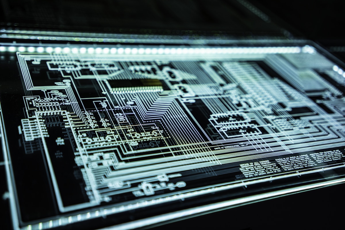
For over five decades, the semiconductor industry has followed Moore’s Law, doubling transistor density approximately every two years. This progress has been driven by advancements in photolithography—the process of using light to pattern circuits onto silicon wafers. As the industry approaches the 2nm node, the current standard, Low-NA Extreme Ultraviolet (EUV) lithography, is reaching its physical resolution limits. The introduction of High-NA (Numerical Aperture) EUV lithography represents the next technical transition in semiconductor manufacturing.
Numerical aperture measures the ability of an optical system to gather and focus light. In EUV lithography, increasing the NA enables finer resolution, allowing manufacturers to print smaller features without the immediate requirement for complex multi-patterning techniques that can impact yield.
The Mechanics of Low-NA EUV (0.33 NA)
Current EUV systems, such as the ASML Twinscan NXE:3400 and 3600 series, utilize a numerical aperture of 0.33. These machines operate using light with a wavelength of 13.5 nanometers. Based on Rayleigh’s Criterion, a 0.33 NA system has a physical resolution limit of approximately 13nm for a single exposure.
For the 7nm and 5nm nodes, Low-NA EUV replaced Deep Ultraviolet (DUV) immersion lithography. However, as features shrink toward the 2nm threshold, 0.33 NA systems require EUV multi-patterning. This process involves splitting a single layer into two or more masks and printing them in successive steps. While effective, multi-patterning increases production time and raises the risk of overlay errors, which contributes to higher costs per wafer.
Defining High-NA EUV (0.55 NA)
High-NA EUV lithography, implemented in ASML’s Twinscan EXE:5000 and EXE:5200 series, increases the numerical aperture to 0.55. This adjustment improves the theoretical resolution limit to approximately 8nm. This capability allows for the single-exposure printing of features required for advanced logic nodes.
The technical innovation in High-NA systems is the anamorphic lens design. Unlike Low-NA systems, High-NA optics provide different magnification levels in the X and Y directions (4x and 8x respectively). This design is necessary to accommodate the larger angles of light required by the 0.55 NA without increasing reticle size. Consequently, the field size is reduced to half that of a standard Low-NA exposure, requiring new strategies for pattern stitching and chip design.
High-NA EUV vs Low-NA EUV: Key Comparisons
1. Resolution and Patterning Complexity
The primary advantage of High-NA EUV is the return to single-exposure patterning for critical layers. For interconnect pitches that require double-patterning on a Low-NA system, a High-NA system can achieve the same result in a single pass. This reduction in process steps is intended to improve cycle times and long-term yields.
2. Throughput and Productivity
High-NA systems utilize higher stage speeds to compensate for the smaller field size. ASML’s EXE:5200 is designed to process over 220 wafers per hour (wph), maintaining parity with high-end Low-NA systems. The throughput advantage is most significant when a single High-NA exposure replaces a Low-NA multi-patterning flow, eliminating the overhead of additional lithography cycles.
3. Economic Considerations and CAPEX
The transition to High-NA requires significant capital expenditure. Industry estimates place the cost of a single High-NA EUV system at approximately $350 million to $400 million, compared to approximately $150 million to $200 million for Low-NA systems. Manufacturers must evaluate these costs against the operational savings achieved by reducing multi-patterning steps.
4. Ecosystem Readiness: Resists and Masks
High-NA requires advancements in materials science. Due to the shallower depth of focus in 0.55 NA systems, photoresist layers must be thinner. To mitigate stochastic defects—random variations at the nanoscale—new metal-oxide resists (MOR) are being developed to replace traditional chemically amplified resists (CAR), providing improved sensitivity and lower defect rates.
Foundry Adoption Landscape
Intel has been an early adopter of High-NA EUV, receiving the first EXE:5000 system for its R&D facilities. Intel plans to integrate High-NA into its upcoming process nodes to achieve density leadership. Other major foundries, including TSMC and Samsung, are evaluating the integration of High-NA systems based on cost-benefit analyses, with broader industry adoption expected as 2nm and sub-2nm production scales.
The Future of Semiconductor Scaling
The shift to High-NA EUV is a fundamental hardware transition for the semiconductor industry. While Low-NA EUV will continue to be used for less critical layers, High-NA will be utilized for the densest layers of logic and memory. The ability to print features with 8nm resolution in a single exposure is a defining factor for the next generation of high-performance computing and mobile processors.
Sources
- ASML Holding N.V. - "High-NA EUV: The Next Step in Lithography Roadmap" (2024).
- IMEC - "The Path to Sub-2nm: Lithography and Materials Challenges" (2023).
- IEEE Spectrum - "How High-NA EUV Will Shrink the Future of Chips" (2024).
- SemiEngineering - "The Economics of 0.55 NA EUV vs. 0.33 NA Multi-Patterning" (2023).
This article was AI-assisted and reviewed for factual integrity.
Photo by Unsplash on Unsplash
Post a Comment